FPGA: Field-Programmable Gate Array
This article introduces the Field-Programmable Gate Array (FPGA), and products of Xilinx and Altera.
What’s FPGA?
A Field-Programmable Gate Array (FPGA) is an integrated circuit designed to be confidgured by a customer or a designer after manufacturing – hence field-programmable. The FPGA configuration is generally specified using a Hardware Description Language (HDL), similar to that used for an Application-Specific Integrated Circuit (ASIC). (Circuit diagrams were previously used to specify the configuration, as they were for ASICs, but this is increasingly rare.)
FPGAs contain an array of programmable logic blocks, and a hierarchy of reconfigurable interconnects that allow the logic blocks to be wired together, like many logic gates that can be inter-wired in different configurations. Logic blocks can be configured to perform complex combinational functions, or merely simple logic gates like AND and XOR. In most FPGAs, logic blocks also include memory elements, which may be simple flip-flops or more complete blocks of memory.
FPGAs are programmable semiconductor devices that are based around a matrix of Configurable Logic Blocks (CLBs) connected through programmable interconnects. FPGAs can be programmed to the desired application or functionality requirements. – Xilinx
Composition of FPGA
-
CLB (Configurable Logic Block)
CLB contains clusters of LUTs, Registers, Arithmetic and other circuitry.
-
LUT (Look-UP Table)
LUT is a hardware implementation of a truth table.
Types of FPGA
- One-Time Programmable (OTP) FPGAs
- SRAM-based FPGAs, which can be reprogrammed as the design evolves
Hard Core & Soft Core
-
Hard Core
- Speed up to 1GHz+
- Can achieve much faster processing speeds
- Fixed and cannot be modified (dedicated silicon area on FPGA)
- Examples: PowerPC used in Virtex-4/5, ARM Cortex-A9 dual-core MCU used in Zynq-7000 All Programmable SoC from Xilinx
-
Soft Core
- Simple microcontroller/ful-fledged microprocessor
- Less Speed around 250MHz & limited by the speed of the fabric
- Can be easily modified and tuned to specific requirements, more features, custom instructions, etc
- Example: LEON3, OpenRISC, MicroBlaze+PicoBlaze, Nios II
A soft-core processor is a microprocessor fully described in softare, usually in an HDL, which can be synthesized in Programmable hardware, such as FPGAs.
Hardware Description Language (HDL)
-
Verilog HDL
IEEE Std. 1364-1995
-
VHDL
IEEE Std. 1076-1993
Xilinx Products
Refer to http://www.xilinx.com/products/silicon-devices/fpga.html
Altera Products
2015-06-01,英特尔宣布以167亿美元收购Altera. 2015-12-28,英特尔完成收购Altera.
Stratix series
The description of Stratix series FPGAs & SoCs can be found on here.
A Stratix FPGA can provide up to 80K logic elements (LEs) and 7.3 Mbits of on-chip RAM arranged in TriMatrix memory blocks, operating at up to 350 MHz. The Stratix FPGA supports external memory interfaces such as DDR SDRAM at 400 Mbps and QDRII SRAM at 800 Mbps. The Stratix FPGA also introduced the world’s first digital signal processing (DSP) block, containing four 18 x 18 multipliers, accumulators, and a summation unit.
Building on the Stratix FPGA high-performance architectural features, the Stratix GX FPGA is the first programmable logic device to incorporate high-speed serial transceivers operating at multi-gigabit speeds. Using a transceiver block supporting four full-duplex channels and clock data recovery (CDR) technology allows transmission of data in excess of 3.1875-Gbps per channel. This data rate supports many common high-speed communication protocols including SerialLite, Gigabit Ethernet, 10-Gigabit Ethernet/XAUI, SONET/SDH, Fibre Channel, the Serial RapidIO® standard, PCI Express, SFI-5, and SPI-5.
| Family | Year of introduction | Process technology |
|---|---|---|
| Stratix | 2002 | 130 nm |
| Stratix GX | 2003 | 130 nm |
| Stratix II | 2004 | 90 nm |
| Stratix II GX | 2005 | 90 nm |
| Stratix III | 2006 | 65 nm |
| Stratix IV | 2008 | 40 nm |
| Stratix V | 2010 | 28 nm |
| Stratix 10 | 2013 | 14 nm Tri-Gate |
Arria series
The description of Arria series FPGAs & SoCs can be found on here.
Altera’s Arria® family delivers optimal performance and power efficiency in the midrange. The Arria family has a rich feature set of memory, logic, and digital signal processing (DSP) blocks combined with the superior signal integrity of up to 28.05 Gbps transceivers that allow you to integrate more functions and maximize system bandwidth. Furthermore, the SoC variants in the Arria V and Arria 10 device families offer an ARM®-based hard processor system (HPS) for even higher integration and power savings.
| Family | Year of introduction | Process technology |
|---|---|---|
| Arria GX | 2007 | 90 nm |
| Arria II GX | 2009 | 40 nm |
| Arria II GZ | 2010 | 40 nm |
| Arria V GX, GT, SX | 2011 | 28 nm |
| Arria V GZ | 2012 | 28 nm |
| Arria 10 GX, GT, SX | 2013 | 20 nm |
Cyclone Series
The description of Cyclone series FPGAs & SoCs can be found on here.
The Cyclone® FPGA series is built to meet your low-power, cost-sensitive design needs, enabling you to get to market faster. Each generation of Cyclone FPGAs solves your technical challenges of increased integration, increased performance, lower power, and faster time to market while meeting your cost-sensitive requirements.
| Family | Year of introduction | Process technology |
|---|---|---|
| Cyclone FPGA | 2002 | 130 nm |
| Cyclone II FPGA | 2004 | 90 nm |
| Cyclone III FPGA | 2007 | 65 nm |
| Cyclone IV FPGA | 2009 | 60 nm |
| Cyclone V FPGA | 2011 | 28 nm |
MAX 10 Series
The description of MAX 10 series FPGAs can be found on here.
Altera’s new MAX 10 FPGAs revolutionize non-volatile integration by delivering advanced processing capabilities in a low-cost, instant-on, small form factor programmable logic device. By providing instant-on dual-configuration with analog-to-digital converters (ADCs), and full-featured FPGA capabilities, they are optimized for a wide range of high-volume, cost-sensitive applications, including industrial, automotive, and communications.
Refer to MAX 10 Product Table.
Design Software
Altera provides a complete suite of development tools for every stage of your design. Whether you are creating a complex FPGA design, writing software for an embedded processor, modeling a digital signal processing (DSP) algorithm, or focusing on system design, Altera has a tool that can help.
-
Tools for FPGA Designers
-
Tools for Software and Embedded Developers
-
Tools for Simulation and Modeling
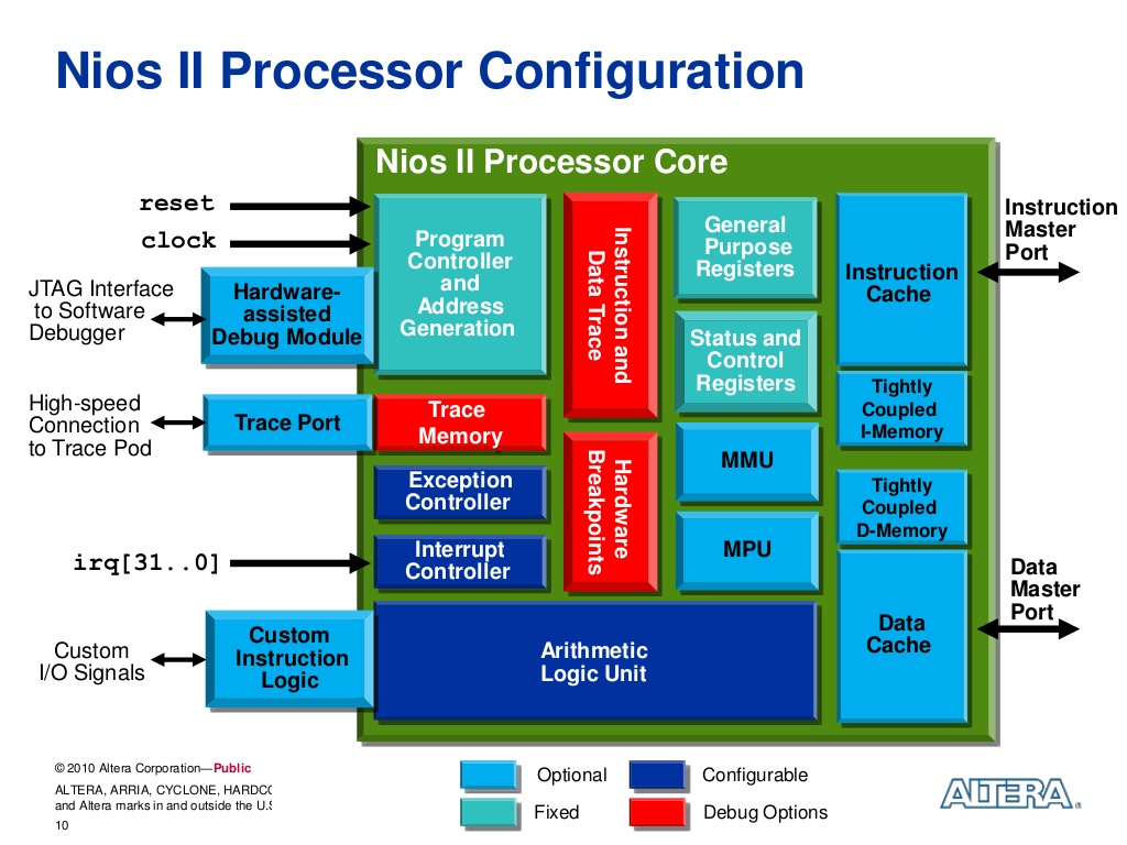
Nios II Embedded Processor
Nios II Embedded Processor Core variants
- Nios II/f Fast Core
- Nios II/s Standard Core
- Nios II/e Economy Core
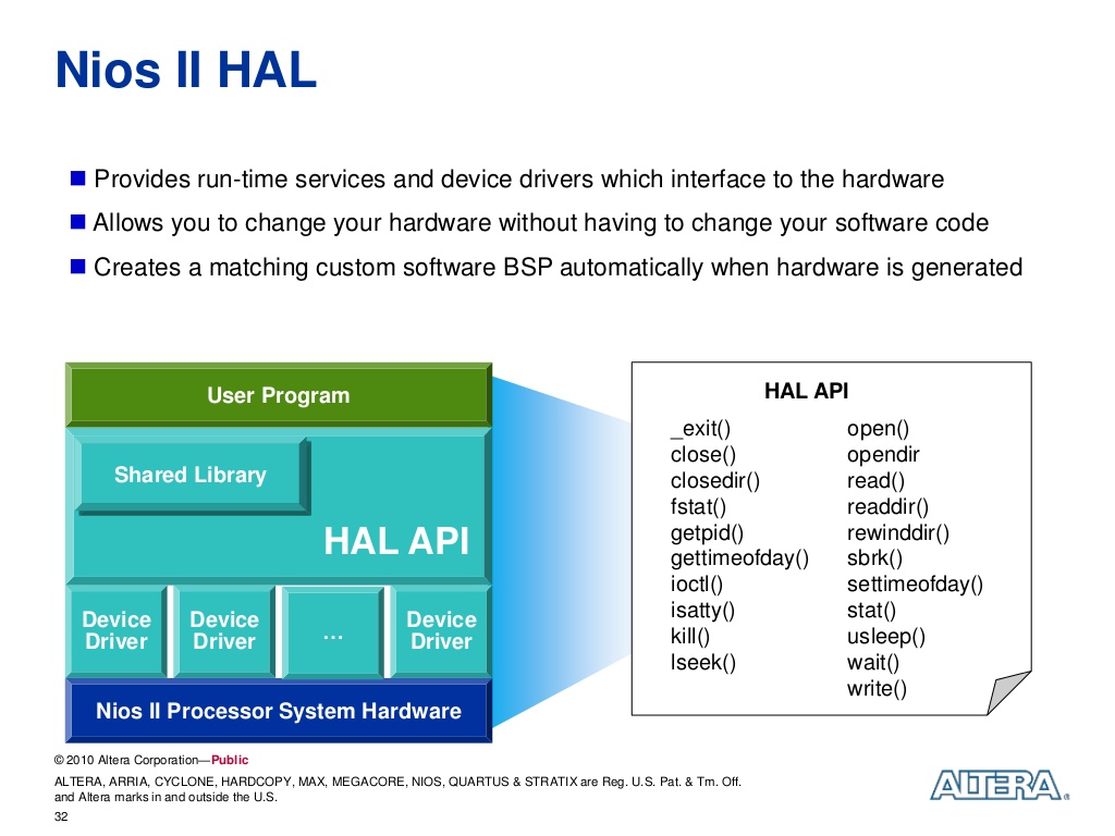
Overview of Nios II Embedded Processor
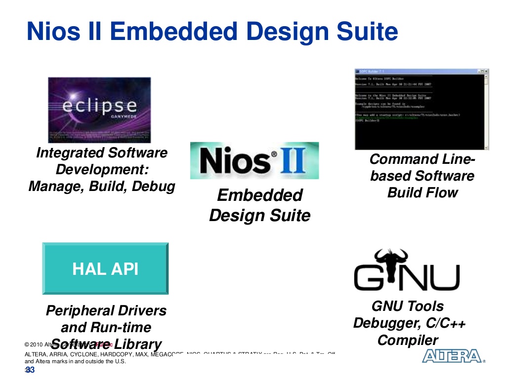
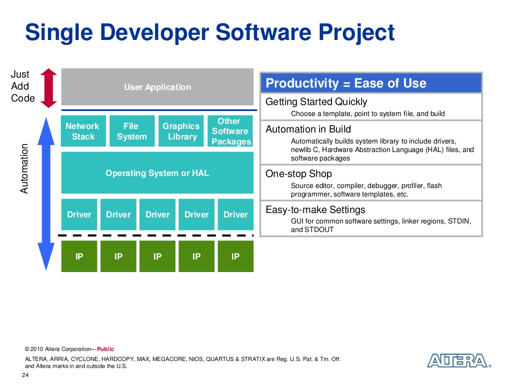
Nios II Embedded Design Suite
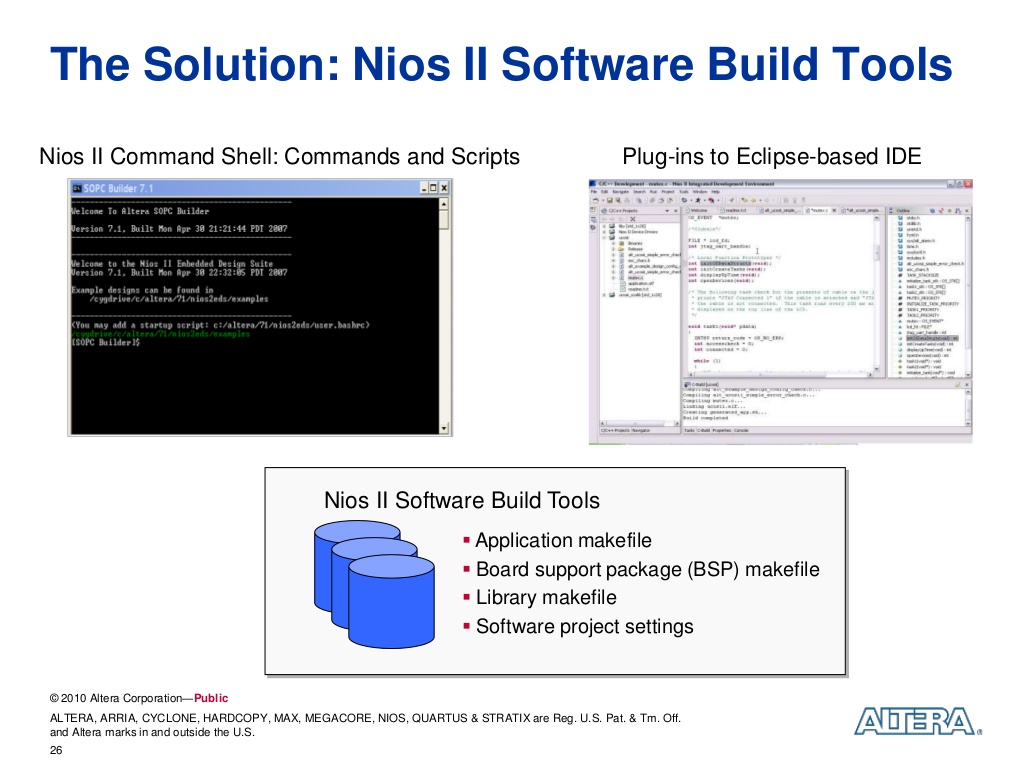
Nios II Software Build Tools
Embedded Development Flow
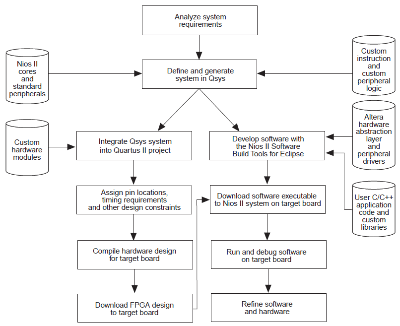
According to Nios II Hardware Development Tutorial, the Nios II development flow consists of three types of development:
- hardware design steps
- software design steps
- system design steps, which involves both hardware and software
For simpler Nios II systems, one person might perform all steps. For more complex systems, separate hardware and software designers might be responsible for different steps. System design steps involve both the hardware and software, and might require input from both sides. In the case of separate hardware and software teams, it is important to know exactly what files and information must be passed between teams at the points of intersection in the design flow.