JTAG: Joint Test Action Group
This article introduces the JTAG (Joint Test Action Group).
Overview
The Joint Test Action Group (JTAG) is an electronics industry association formed in 1985 for developing a method of verifying designs and testing printed circuit boards after manufacture. In 1990 the Institute of Electrical and Electronics Engineers (IEEE) codified the results of the effort in IEEE Standard 1149.1-1990, entitled Standard Test Access Port and Boundary-Scan Architecture.
In the same year, Intel released their first processor with JTAG (the 80486) which led to quicker industry adoption by all manufacturers. In 1994, a supplement that contains a description of the boundary scan description language (BSDL) was added. Further refinements regarding the use of all-zeros for EXTEST, separating the use of SAMPLE from PRELOAD and better implementation for OBSERVE_ONLY cells were made and released in 2001.[4] Since 1990, this standard has been adopted by electronics companies around the world. Boundary scan is now mostly synonymous with JTAG, but JTAG has essential uses beyond such manufacturing applications.
Electrical Characteristics
A JTAG interface is a special interface added to a chip. Depending on the version of JTAG, two, four, or five pins are added. The four and five pin interfaces are designed so that multiple chips on a board can have their JTAG lines daisy-chained together if specific conditions are met. The two pin interface is designed so that multiple chips can be connected in a star topology. In either case a test probe need only connect to a single “JTAG port” to have access to all chips on a circuit board.
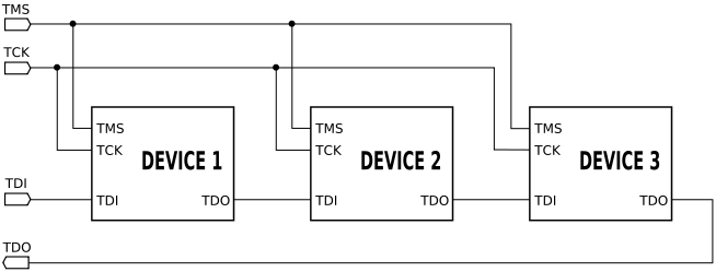
Daisy-chained JTAG (IEEE 1149.1)
The connector pins are
- TDI (Test Data In)
- TDO (Test Data Out)
- TCK (Test Clock)
- TMS (Test Mode Select)
- TRST (Test Reset) optional
The TRST pin is an optional active-low reset to the test logic - usually asynchronous, but sometimes synchronous, depending on the chip. If the pin is not available, the test logic can be reset by switching to the reset state synchronously, using TCK and TMS. Note that resetting test logic doesn’t necessarily imply resetting anything else. There are generally some processor-specific JTAG operations which can reset all or part of the chip being debugged.
Since only one data line is available, the protocol is serial. The clock input is at the TCK pin. One bit of data is transferred in from TDI, and out to TDO per TCK rising clock edge. Different instructions can be loaded. Instructions for typical ICs might read the chip ID, sample input pins, drive (or float) output pins, manipulate chip functions, or bypass (pipe TDI to TDO to logically shorten chains of multiple chips).
As with any clocked signal, data presented to TDI must be valid for some chip-specific Setup time before and Hold time after the relevant (here, rising) clock edge. TDO data is valid for some chip-specific time after the falling edge of TCK.
The maximum operating frequency of TCK varies depending on all chips in the chain (the lowest speed must be used), but it is typically 10-100 MHz (100-10 ns per bit). Also TCK frequencies depend on board layout and JTAG adapter capabilities and state. One chip might have a 40 MHz JTAG clock, but only if it is using a 200 MHz clock for non-JTAG operations; and it might need to use a much slower clock when it is in a low power mode. Accordingly, some JTAG adapters have adaptive clocking using an RTCK (Return TCK) signal. Faster TCK frequencies are most useful when JTAG is used to transfer lots of data, such as when storing a program executable into flash memory.
Clocking changes on TMS steps through a standardized JTAG state machine. The JTAG state machine can reset, access an instruction register, or access data selected by the instruction register.
JTAG platforms often add signals to the handful defined by the IEEE 1149.1 specification. A System Reset (SRST) signal is quite common, letting debuggers reset the whole system, not just the parts with JTAG support. Sometimes there are event signals used to trigger activity by the host or by the device being monitored through JTAG; or, perhaps, additional control lines.
Even though few consumer products provide an explicit JTAG port connector, the connections are often available on the printed circuit board as a remnant from development prototyping and/or production. When exploited, these connections often provide the most viable means for reverse engineering.
Q: Under what conditions can I daisy-chain JTAG?
A: This isn’t an easy questions to answer, because a lot of conditions have to be met here. First of all every IC in your chain must be electrically compatible with JTAG pins. Check the datasheet to see if your ICs meet this condition. The JTAG communication speed must be low enough even for the slowest IC, which means that if you need a high-speed JTAG but you include some very slow part in your chain, it will degrade throughput of JTAG chain dramatically and could make the debugging or programming impossible.
Another problem will occur with “extended” JTAG pins such as nTRST/nSRST/DBGRQ/etc. These pins cannot be multiplexed and only one IC can provide them (for example connecting up multiple nSRST pins together would reset all such ICs on your board).
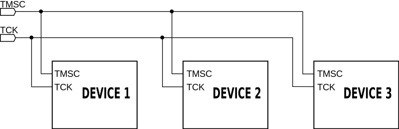
Reduced pin count JTAG (IEEE 1149.7)
Reduced pin count JTAG uses only two wires, a clock wire and a data wire. This is defined as part of the IEEE 1149.7 standard. The connector pins are
- TMSC (Test Serial Data)
- TCKC (Test Clock)
It is called cJTAG for compact JTAG.
The two wire interface reduced pressure on the number of pins, and devices can be connected in a star topology. The star topology enables some parts of the system to be powered down, while others can still be accessed over JTAG; a daisy chain requires all JTAG interfaces to be powered. Other two-wire interfaces exist, such as Serial Wire Debug.
Communications Model
In JTAG, devices expose one or more test access ports (TAPs). The picture above shows three TAPs, which might be individual chips or might be modules inside one chip. A daisy chain of TAPs is called a scan chain, or (loosely) a target. Scan chains can be arbitrarily long, but in practice twenty TAPs is unusually long.
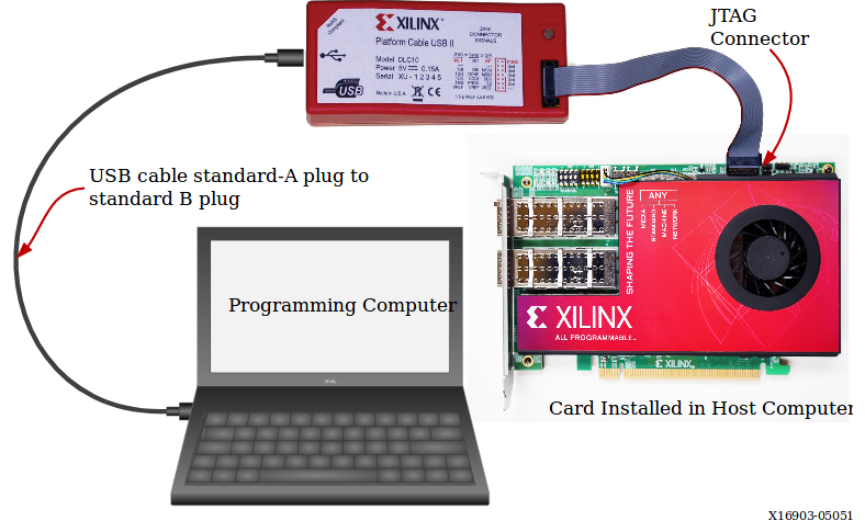
To use JTAG, a host is connected to the target’s JTAG signals (TMS, TCK, TDI, TDO, etc.) through some kind of JTAG adapter, which may need to handle issues like level shifting and galvanic isolation. The adapter connects to the host using some interface such as USB, PCI, Ethernet, and so forth.
Client Support
The target’s JTAG interface is accessed using some JTAG-enabled application and some JTAG adapter hardware. There is a wide range of such hardware, optimized for purposes such as production testing, debugging high speed systems, low cost microcontroller development, and so on. In the same way, the software used to drive such hardware can be quite varied. Software developers mostly use JTAG for debugging and updating firmware.
If you want to acquire a JTAG adapter, you first need to decide what systems it must support. Everything else follows from that, including your software options. Low-end adapters may cost less than $US 50 and have limited hardware and software support. High-end adapters can cost a hundred times as much, including software support, and have corresponding improvements in capability.
Connectors
There are no official standards for JTAG adapter physical connectors. Development boards usually include a header to support preferred development tools; in some cases they include multiple such headers, because they need to support multiple such tools. For example, a microcontroller, FPGA, and ARM application processor rarely shares tools, so a development board using all of those components might have three or more headers. Production boards may omit the headers; or when space is tight, just provide JTAG signal access using test points.
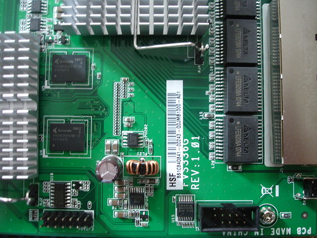
A Netgear FVS336G firewall with a 14 pin JTAG header at lower left:
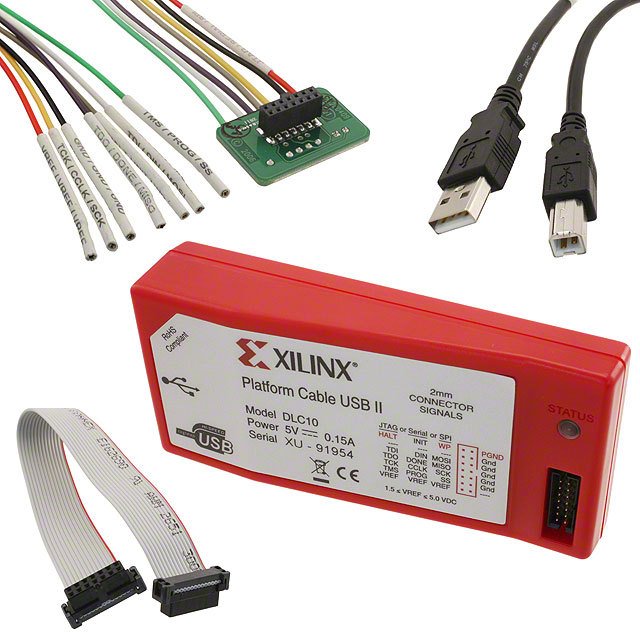
Adapter hardware
Adapter hardware varies widely. When not integrated into a development board, it involves a short cable to attach to a JTAG connector on the target board; a connection to the debugging host, such as a USB, PCI, or Ethernet link; and enough electronics to adapt the two communications domains (and sometimes provide galvanic isolation). A separate power supply may be needed. There are both “dumb” adapters, where the host decides and performs all JTAG operations; and “smart” ones, where some of that work is performed inside the adapter, often driven by a microcontroller. The “smart” adapters eliminate link latencies for operation sequences that may involve polling for status changes between steps, and may accordingly offer faster throughput.
As of 2009, adapters with full speed USB links are probably the most common approach, and new products often include high speed USB support. Higher end products often support Ethernet, with the advantage that the debug host can be quite remote. Adapters which support high speed trace ports generally include several megabytes of trace buffer and provide high speed links (USB or Ethernet) to get that data to the host.
Personal computer parallel port adapters are simple and inexpensive, but they are relatively slow because they use the host CPU to change each bit (“bit banging”). They have declined in usefulness because newer computers do not have parallel port hardware. Driver support is also a problem, because the adapter electronics varied so widely.
Serial port adapters also exist, and are similarly declining in usefulness. They generally involve either slower bit banging than a parallel port, or a microcontroller translating some command protocol to JTAG operations. Such serial adapters are also not fast, but their command protocols could generally be reused on top of higher speed links.
With all JTAG adapters, software support is a basic concern. Many vendors do not publish the protocols used by their JTAG adapter hardware, limiting their customers to the tool chains supported by those vendors. This is a particular issue for “smart” adapters, some of which embed significant amounts of knowledge about how to interact with specific CPUs.
Software development
Most development environments for embedded software include JTAG support. There are, broadly speaking, three sources of such software:
-
Chip Vendors may provide the tools, usually requiring a JTAG adapter they supply. Examples include FPGA vendors such as Xilinx and Altera, Atmel for its AVR8 and AVR32 product lines, and Texas Instruments for most of its DSP and micro products. Such tools tend to be highly featured, and may be the only real option for highly specialized chips like FPGAs and DSPs. Lower end software tools may be provided free of charge. The JTAG adapters themselves are not free, although sometimes they are bundled with development boards.
-
Tool Vendors may supply them, usually in conjunction with multiple chip vendors to provide cross-platform development support. ARM-based products have a particularly rich third party market, and a number of those vendors have expanded to non-ARM platforms like MIPS and PowerPC. Tool vendors sometimes build products around free software like GCC and GDB, with GUI support frequently using Eclipse. JTAG adapters are sometimes sold along with support bundles.
-
Open Source tools exist. As noted above, GCC and GDB form the core of a good toolchain, and there are GUI environments to support them.
All such software tends to include basic debugger support: stopping, halting, single stepping, breakpoints, data structure browsing, and so on. Commercial tools tend to provide tools like very accurate simulators and trace analysis, which are not currently available as open source.
References
- JTAG on zh.wikipedia.org
- JTAG on en.wikipedia.org
- What is JTAG
- Boundary-Scan Information Site
- JTAG FAQ
- IEEE Std 1149.1 (JTAG) Testability