JESD204
This article introduces the JESD204.
Overview
According to JESD204 Serial Interface and JEDEC Standard Data Converters, the JESD204 and the JESD204B revision data converter serial interface standard was created through the JEDEC committee to standardize and reduce the number of data inputs/outputs between high-speed data converters and other devices, such as FPGAs (field-programmable gate arrays). Fewer interconnects simplifies layout and allows smaller form factor realization without impacting overall system performance. These attributes are important to address the system size and cost constraints of a range of high speed ADC applications, including wireless infrastructure (GSM, EDGE, W-CDMA, LTE, CDMA2000, WiMAX, TD-SCDMA) transceiver architectures, software-defined radios, portable instrumentation, medical ultrasound equipment, and Mil/Aero applications such as radar and secure communications. Analog Devices is an original participating member of the JEDEC JESD204 standards committee and we have concurrently developed compliant data converter technology and tools, and a comprehensive product roadmap to fully enable our customers to take advantage of this significant interfacing breakthrough.
JESD204 Standards
According to JESD204B Survival Guide, the JESD204 interface brings this efficiency and offers several advantages over its CMOS and LVDS predecessors in terms of speed, size, and cost. Designs employing JESD204 enjoy the benefits of a faster interface to keep pace with the faster sampling rates of converters. In addition, there is a reduction in pin count which leads to smaller package sizes and a lower number of trace routes that make board designs much easier and offers lower overall system cost. The standard is also easily scalable so it can be adapted to meet future needs. This has already been exhibited by the two revisions that the standard has undergone. The JESD204 standard has seen two revisions since its introduction in 2006 and is now at revision B. As the standard has been adopted by an increasing number of converter vendors and users as well as FPGA manufacturers, it has been refined and new features have been added that have increased efficiency and ease of implementation. The standard applies to both analog to digital converters (ADCs) as well as digital to analog converters (DACs) and is primarily intended as a common interface to FPGAs (but may also be used with ASICs).
JESD204 General
In April of 2006, the original version of JESD204 was released. The standard describes a multigigabit serial data link between converter(s) and a receiver, commonly a device such as an FPGA or ASIC. In this original version of JESD204, the serial data link was defined for a single serial lane between a converter or multiple converters and a receiver. A graphical representation is provided in the following figure:
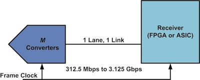
The lane shown is the physical interface between M number of converters and the receiver which consists of a differential pair of interconnect utilizing current mode logic (CML) drivers and receivers. The link shown is the serialized data link that is established between the converter(s) and the receiver. The frame clock is routed to both the converter(s) and the receiver and provides the clock for the JESD204 link between the devices.
The lane data rate is defined between 312.5 Megabits per second (Mbps) and 3.125 Gigabits per second (Gbps) with both source and load impedance defined as 100 Ω ±20%. The differential voltage level is defined as being nominally 800 mV peak-to-peak with a common mode voltage level range from 0.72 V to 1.23 V. The link utilizes 8b/10b encoding which incorporates an embedded clock, removing the necessity for routing an additional clock line and the associated complexity of aligning an additional clock signal with the transmitted data a high data rates. It became obvious as the JESD204 standard began being used that the standard needed to be revised to incorporate support for multiple aligned serial lanes with multiple converters to accommodate increasing speeds and resolutions of converters.
JESD204A
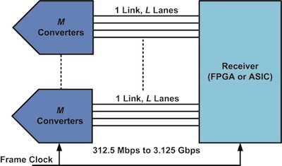
This realization led to the first revision of the JESD204 standard in April of 2008 which became known as JESD204A. This revision of the standard added the ability to support multiple aligned serial lanes with multiple converters. The lane data rates, supporting from 312.5 Mbps up to 3.125 Gbps remained unchanged as did the frame clock and the electrical interface specifications. Increasing the capabilities of the standard to support multiple aligned serial lanes made it possible for converters with high sample rates and high resolutions to meet the maximum supported data rate of 3.125 Gbps. The following figure shows a graphical representation of the additional capabilities added in the JESD204A revision to support multiple lanes:
JESD204B
Although both the original JESD204 standard and the revised JESD204A standard were higher performance than legacy interfaces, they were still lacking a key element. This missing element was deterministic latency in the serialized data on the link.
When dealing with a converter, it is important to know the timing relationship between the sampled signal and its digital representation in order to properly recreate the sampled signal in the analog domain once the signal has been received (this situation is, of course for an ADC, a similar situation is true for a DAC). This timing relationship is affected by the latency of the converter which is defined for an ADC as the number of clock cycles between the instant of the sampling edge of the input signal until the time that its digital representation is present at the converter’s outputs. Similarly, in a DAC, the latency is defined as the number of clock cycles between the time the digital signal is clocked into the DAC until the analog output begins changing. In the JESD204 and JESD204A standards, there were no defined capabilities that would deterministically set the latency of the converter and its serialized digital inputs/outputs.
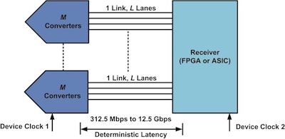
In addition, converters were continuing to increase in both speed and resolution. These factors led to the introduction of the second revision of the standard, JESD204B. In July of 2011, the second and current revision of the standard, JESD204B, was released. One of the key components of the revised standard was the addition of provisions to achieve deterministic latency. In addition, the data rates supported were pushed up to 12.5 Gbps broken down into different speed grades of devices. This revision of the standard calls for the transition from using the frame clock as the main clock source to using the device clock as the main clock source. The following figure gives a representation of the additional capabilities added by the JESD204B revision:
In the previous two versions of the JESD204 standard, there were no provisions defined to ensure deterministic latency through the interface. The JESD204B revision remedies this issue by providing a mechanism to ensure that, from power-up cycle to power-up cycle and across link re-synchronization events, the latency should be repeatable and deterministic. One way this is accomplished is by initiating the initial lane alignment sequence in the converter(s) simultaneously across all lanes at a well-defined moment in time by using an input signal called SYNC~.
Another implementation is to use the SYSREF signal which is a newly defined signal for JESD204B. The SYSREF signal acts as the master timing reference and aligns all the internal dividers from device clocks as well as the local multi-frame clocks in each transmitter and receiver. This helps to ensure deterministic latency through the system. The JESD204B specification calls out three device sub-classes:
- Sub-class 0: No support for deterministic latency. Sub-class 0 can simply be compared to a JESD204A link.
- Sub-class 1: Deterministic latency using SYSREF. Sub-class 1 is primarily intended for converters operating at or above 500MSPS.
- Sub-class 2: Deterministic latency using SYNC~. Sub-class 2 is primarily for converters operating below 500MSPS.
In addition to the deterministic latency, the JESD204B version increases the supported lane data rates to 12.5 Gbps and divides devices into three different speed grades. The source and load impedance is the same for all three speed grades being defined as 100 Ω ±20%.
- The first speed grade aligns with the lane data rates from the JESD204 and JESD204A versions of the standard and defines the electrical interface for lane data rates up to 3.125 Gbps.
- The second speed grade in JESD204B defines the electrical interface for lane data rates up to 6.375 Gbps. This speed grade lowers the minimum differential voltage level to 400 mV peak-to-peak, down from 500 mV peak-to-peak for the first speed grade.
- The third speed grade in JESD204B defines the electrical interface for lane data rates up to 12.5 Gbps. This speed grade lowers the minimum differential voltage level required for the electrical interface to 360 mV peak-to-peak. As the lane data rates increase for the speed grades, the minimum required differential voltage level is reduced to make physical implementation easier by reducing required slew rates in the drivers.
To allow for more flexibility, the JESD204B revision transitions from the frame clock to the device clock. Previously, in the JESD204 and JESD204A revisions, the frame clock was the absolute timing reference in the JESD204 system. Typically, the frame clock and the sampling clock of the converter(s) were usually the same. This did not offer a lot of flexibility and could cause undesired complexity in system design when attempting to route this same signal to multiple devices and account for any skew between the different routing paths. In JESD204B, the device clock is the timing reference for each element in the JESD204 system. Each converter and receiver receives their respective device clock from a clock generator circuit which is responsible for generating all device clocks from a common source. This allows for more flexibility in the system design, but it requires that the relationship between the frame clock and device clock be specified for a given device.
JESD204C
Devices
References
- JESD204 Serial Interface and JEDEC Standard Data Converters
- JESD204B Survival Guide
- JESD204B Overview
- Ready to make the jump to JESD204B?
- When is the JESD204B interface the right choice?